[Thin Film Part3] Plasma Basics

Welcome back to the "Thin Film Series," where we delve into the fundamental materials and processes crucial to semiconductor device fabrication. In this third episode, "Plasma Basics," we explore the fascinating world of plasma, a critical player in semiconductor manufacturing techniques such as CVD, PVD, and dry etching. This episode is designed to provide a comprehensive understanding of plasma fundamentals and their applications in the semiconductor industry. By the end of this video, you'll have a solid foundation in plasma basics, recognizing its indispensable role in the development of semiconductor components. Whether you're an aspiring engineer, a dedicated semiconductor enthusiast, or an experienced industry professional, this video will enhance your knowledge and insight into the dynamic field of plasma technology. Don't forget to like, subscribe, and turn on notifications to stay updated with our educational content. Below are the chapters of this video. Click on any timestamp to directly access the desired section.
Episode Outline:
1. Introduction to Nonthermal Plasma in Semiconductor Processes
[0:00] Intro: Setting expectations for this episode.
[1:03] Early Discoveries: Tracing plasma's recognition from Crookes Tube to Irving Langmuir's naming analogy.
[3:05] Ubiquity of Plasma: Its prevalence in the universe and natural phenomena.
[4:59] Plasma in Nature: Observing plasma in everyday life from candle flames to celestial events.
[6:34] Visualizing Plasma: The science behind plasma's colorful glow.
[8:21] Significance in Industry: The role of lowtemperature, nonthermal plasma in semiconductor manufacturing.
[10:41] Plasma Composition: Components of plasma and their importance in maintaining quasineutrality.
2. DC Plasma and DC Magnetron Sputtering
[14:53] Generating DC Plasma: Mechanics of plasma glow in a gas discharge tube with a DC power supply.
[16:41] Townsend Avalanche: The process of electron multiplication in DC plasma.
[18:28] Characteristics of Glow Discharge: Analyzing plasma behavior in different sections of a discharge tube.
[20:32] DC Magnetron Sputtering: Application in thin film deposition and its limitations for insulating targets.
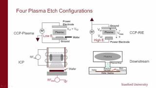
3. RF Plasma: CCP vs ICP
[24:11] Plasma Oscillation & Frequencies: How plasma oscillates at different frequencies.
[25:50] RFPlasma Interactions: Dynamics of radio frequency interactions with plasma.
[27:29] Sustaining RF Plasma: Coupling mechanisms in Capacitively Coupled Plasma (CCP) and Inductively Coupled Plasma (ICP).
[29:22] Understanding CCP: Formation and effects of sheath in CCP.
[30:46] Electrode Effects in CCP: Varied applications based on electrode area ratios.
[32:17] ICP Mechanisms: Inductive coupling and skin depth considerations.
[34:17] Comparing Plasma Sources: Differences between DC, CCP, and ICP technologies.
4. Advanced Plasma Technologies in Semiconductor Processing
[36:23] Innovative Approaches: Microwave and Electron Cyclotron Resonance (ECR) Plasma applications.
![[Thin Film Part4] PVD Basics](https://i.ytimg.com/vi/evpHv8o6kno/mqdefault.jpg)


![[Thin Film Part1] Stress and Strain](https://i.ytimg.com/vi/45_gbTY_9w4/mqdefault.jpg)