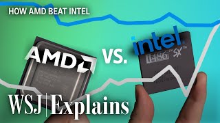
What's inside Intel Pentium Pro Processor chip
@MakeGold
The Intel Pentium Pro processor, released in 1995, was a significant advancement in its time. While its technology might seem outdated compared to modern CPUs, understanding its internal components can offer valuable insights into the evolution of processor design. Here's a breakdown of what was inside a Pentium Pro chip
Central Processing Unit (CPU) Die
Execution Units: The Pentium Pro had six execution units: two integer units, one floatingpoint unit (FPU), a load unit, store address unit, and a store data unit. These units handled different processing tasks like calculations, data movement, and memory access.
Cache: It incorporated two levels of cache:
L1 cache: 8 or 16 Kilobyte (separate for data and instructions) stored frequently used data close to the execution units for faster access.
L2 cache: Located on a separate die, it offered a larger capacity of 256 Kilobyte, 512 Kilobyte, or even 1megabyte further reducing main memory access latency.
Microprocessor Core: Built on a 0.50 micrometer or 0.35 micrometer BiCMOS process, it housed the transistors and logic circuits responsible for core processing tasks.
Package
Ceramic MultiChip Module (MCM): The Pentium Pro wasn't a single chip but two dies housed in a ceramic MCM. One die held the CPU core, and the other contained the L2 cache.
Socket: It used Socket 8, a specific connector interface compatible with motherboards designed for this processor.
FrontSide Bus: This bus connected the processor to the main memory and chipset, operating at 60 or 66 MHz for data transfer.
Clock Crystal: Regulated the internal operating frequency of the processor, typically ranging from 150 to 200 MHz.
Voltage Regulator: Provided the necessary power to various components within the chip.
Overall, the Pentium Pro was a complex and powerful processor for its time, featuring multiple execution units, large L2 cache, and BiCMOS technology. While its internal design wouldn't compare to modern multicore processors, understanding its components gives us a glimpse into the fascinating journey of processor evolution.


