Two-Layer PCB Design Tips: Achieving the Optimal Layout

Learn the secrets of TwoLayer PCB Design with this expert guide from Tech Consultant Zach Peterson. This video dives into the fundamental techniques and strategies essential for achieving an optimal layout in your twolayer PCB projects. This tutorial covers everything from proper grounding and routing to maximizing board efficiency and performance.
Follow along as Zach explores practical examples, demonstrates effective design practices, and answers your most pressing questions.
0:00 Intro
0:35 Example TwoLayer Boards
4:18 Ground Pour for Digital Signals
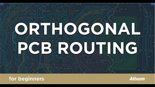
6:31 Orthogonal Routing, Return Paths & Power
14:56 USB Interface?
17:24 Putting It All Together
For more PCB Layout videos, click here: • PCB Layout
For more PCB Design for Intermediate Users videos, click here: • PCB Design for Intermediate Users
For more Tech Consultant Zach Peterson videos, click here: • Technical Consultant Zach Peterson
Can You Route USB 2.0 on a 2Layer Board?: • Can You Route USB 2.0 on a 2Layer Bo...
Routing Requirements for a USB Interface on a 2Layer PCB: https://resources.altium.com/p/routin...
Can You Route Digital Signals on a 2layer PCB Design?: https://resources.altium.com/p/canyo...
The Most Common 2Layer PCB Design Mistakes and How To Avoid Them: • The Most Common 2Layer PCB Design Mi...
Exclusive 15 Days Free Altium Designer Access: https://www.altium.com/promotions/alt...
Don't forget to follow us on social to stay uptodate on the latest Altium Academy content.
Follow Altium on TikTok: / altiumdesigner
Follow Altium on Twitter: / altium
Follow Altium on Linkedin: / altium
Follow Altium on Facebook: / altiumofficial
Ready to try the industry's bestinclass design experience yourself? Download it today and get started! https://www.altium.com/downloads?utm_...
The Altium Academy is an online experience created to bring modern education to PCB Designers and Engineers all across the world. Here you can access a vast library of free training and educational content covering everything from basic design to advanced principles and stepbystep walkthroughs. Join industry legends as they share their career knowledge, review reallife design projects, or learn how to leverage one of Altium's leading design tools. No matter your level of experience, the Altium Academy can help you become a better Designer and Engineer!
About Altium LLC
Altium LLC (ASX:ALU), a global software company based in San Diego, California, is accelerating the pace of innovation through electronics. From individual inventors to multinational corporations, more PCB designers and engineers choose Altium software to design and realize electronicsbased products.
#PCBDesign #TwoLayerPCB #CircuitBoard #ElectronicsDesign #PCBLayout #DIYElectronics #HardwareDesign #TechTutorial #Engineering #CircuitDesign