
KiCad STM32 + RF + USB Hardware Design - Phil's Lab #5

⏵Hardware and PCB design course: https://www.philslab.net/courses
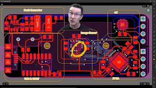
Overview of STM32, RF, and USB hardware design, schematic creation, and PCB layout and routing in KiCad using a realworld example project. (Timestamps in description)
Various tips on controlled impedance routing, differential pairs, USB, and RF layout.
If you're enjoying my content, please consider becoming a patron: / phils94
Correction in schematic: NRF24 IREF pin needs to be pulled low to GND via a 10k resistor (not to 3V3 as shown in the video!). Fix has been pushed to GitHub.
Design files: https://github.com/pms67/STRFKicad
https://jlcpcb.com/RHS
TIMESTAMPS
[Introduction]
00:00 System overview, component selection
03:15 STM32 pinout and peripheral selection
[Schematic]
04:10 Schematic sectioning
04:48 Power supply (power via USB, filtering, USB decoupling caps)
06:45 STM32 microcontroller (USB connections and terminations, SPI, LEDs, decoupling)
09:55 SWD (Serial Wire Debug) connector
10:45 USB connector and ESD protection
13:11 NRF24 RF transceiver
14:40 Extern crystal (load capacitor calculation)
15:57 RF antenna matching circuit
17:31 Component selection and sizing
[Layout]
19:24 Rough layout and sectioning (USB, power, microcontroller, and RF)
20:37 Component placement order (most 'critical' components first)
21:30 USB ESD protection placement
21:42 RF layout
22:16 Determining board outline (size and rounded edges)
22:42 Finetuning the layout
[Routing]
23:24 Layer stackup (4 layer board)
24:16 Sectioning (USB, power, microcontroller, and RF), track widths, and clearance
25:17 Power and ground via connections to copper pours
26:00 Ground and power planes
26:43 Power supply routing
27:26 STM32 routing
28:15 Crystal routing
29:40 RF and USB routing (trace impedance, differential routing, ground pours)
36:53 RF guard ring
38:45 Clearance between traces
39:25 Viainpad
[Silkscreen]
40:05 Labelling and logo
40:40 Marking 'pin 1' locations
40:53 Marking diode polarity
[Manufacturing]
41:42 Checking your work
42:00 Gerber and drill file export
42:25 Footprint positions file (for assembly)
42:49 Bill of materials (BOM)
43:10 Gerber file check (via GerbView)
ID: QIBvbJtYjWuHiTG0uCoK


![[LIVE] How to Achieve Proper Grounding Rick Hartley Expert Live Training (US)](https://i.ytimg.com/vi/ySuUZEjARPY/mqdefault.jpg)