How To Improve Your PCB Layout - Routing u0026 Space

Commenting on a PCB Layout done by a junior engineer.
Links:
Interesting PCB Layout Design Guidelines for Signals above 20Gbps • Interesting PCB Layout Design Guideli...
High Speed PCB Design Rules (Lesson 4 of Advanced PCB Layout Course): • High Speed PCB Design Rules (Lesson 4...
CHAPTERS:
00:00 What is this video about
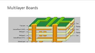
01:10 DDR4 memory layout spacing & length matching
08:19 Differential pair spacing & routing
15:47 NAND interface routing
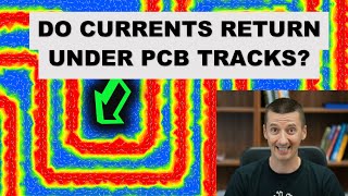
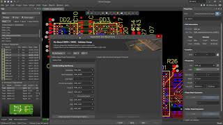
18:21 Track vs Track clearance
20:20 Edge to Track / Component clearance
Would you like to support me in what I do? It's simple:
you will help me a LOT, when you sign up for one of our Schematic and PCB Design online courses at https://www.fedevel.com/academy/
The other ways to support me in what I do are:
Subscribe to this channel
support me through Patreon page / robertferanec
sign up for my Udemy course, Learn to Design Your Own Boards https://www.udemy.com/learntodesign...
send me an email and/or leave a positive comment
watch and like the videos :)
read my Welldone Blog at https://www.fedevel.com/welldoneblog/
spread a word about FEDEVEL Academy
It is much appreciated. Thank you,
Robert