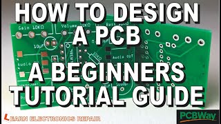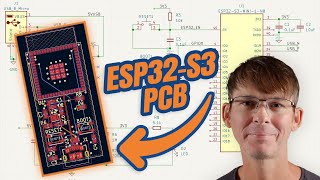
Easy u0026 Quick EasyEDA Tutorial - USB-C Power Supply Design + Box in 2 Hours

In this tutorial you will learn how to draw schematic, do PCB layout, design a box and how to manufacture everything. As an example you will design USBC Power Supply.
How to Make a Custom PCB in 2 Hours | Full Tutorial | EasyEDA
Learn more about electronics, check out our online courses:
https://www.fedevel.com/courses
Chapters:
00:00 What you will create
00:52 Start a new project in EasyEDA
02:50 Adding USBC connector to schematic
04:56 Adding output connector
06:24 Connecting USBC
07:34 Connecting USBC CC1 and CC2 pins
08:23 Adding 5.1k resistors
09:53 Adding 100nF capacitors
11:47 Adding LED
12:54 Adding 1k resistor
14:57 Selecting in EasyEDA
15:43 Naming nets
16:11 Creating your own component Mounting holes
17:51 Creating footprint in EasyEDA
19:24 Adding mounting holes to schematic
20:49 Adding CC pin info into schematic
23:26 Annotating schematic
24:27 Enable support for color PCB silkscreen
24:41 Schematic check Running ERC
24:55 Starting PCB
25:30 Placing big components in PCB (MH, J)
26:35 Define board shape
27:26 Placing small components (R, C, D)
29:12 JLCPCB manufacturing capabilities
29:48 Setting up PCB design rules
30:54 Hide reference designators
31:05 Starting PCB Layout
31:53 Connecting CC pins
32:21 Connecting GND
35:02 Draw DIODE connection
35:20 Making changes in schematic and transferring them to PCB
36:13 Working with polygons (updating, thermal relief)
37:13 Connecting +5V
39:15 Prohibited region
39:57 Place reference designators
41:40 Adding text on silkscreen
46:34 Adding gold logo
48:17 Adding color image on silkscreen
49:28 Starting BOX (enclosure)
51:45 Add openings for connectors
57:11 Add opening for LED
59:13 Adding support for screws
1:03:16 Adding + and signs
1:05:15 Exporting 3D model and 3D printing box
1:07:32 Generating manufacturing outputs
1:08:16 Generating gerber files for color PCB
1:10:43 Replacing color picture with a standard one
1:12:11 Generating gerber files for standard PCB
1:13:45 Generating BOM (Bill of material)
1:14:43 Generating Pick and Place file
1:15:47 Ordering our boards: PCB and Assembly
1:18:23 Ordering box
1:23:19 Finishing ordering
1:24:53 Ordering missing connector
1:26:02 Confirming placement and box manufacturing
1:27:51 Unpacking our boards
1:28:19 Unpacking the 3D printed boxes / enclosures
1:29:09 Inspecting the board, soldering down the missing connector
1:29:52 Measuring our board
1:30:34 Placing board inside of 3D printed box
1:31:05 Testing our board
1:32:11 Thank you very much for watching