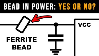
Do you need thick copper layers in PCB for high currents? Are you sure? | Steve Sandler

What is important when designing boards and power supplies with high currents? Explained by Steve Sandler
Links:
Steve's LinkedIn: / stevensandler022a7210
Steve's Online Course: https://marketplace.fedevel.education...
Steve's company: Picotest https://www.picotest.com/
Chapters:
00:00 What is this video about
00:32 Current state of the art
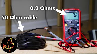
09:20 Why inductance is the biggest challenge (1)
19:15 Minimizing the inductance (1)
20:47 Thinner dielectric for even lower inductance (1)
23:35 Why inductance is the biggest challenge (2)
39:03 Decoupling the ASIC
45:50 Minimizing the inductance (2)
50:55 Thinner dielectric for even lower inductance (2)
53:23 Carrying the current (ANSWER on the question in title)
59:24 Stability Both input and output (control loops)
1:10:45 Million dollar chip
1:17:55 What VRMs can supply this kind of currents?
1:26:20 Is GaN the answer?
1:31:58 Testing gets really tough
1:37:34 Thank you and contact
Would you like to support me? It's simple:
Sign up for online courses hosted on our platform: https://marketplace.fedevel.education/
Sign up for my Hardware design and PCB Layout online courses: https://academy.fedevel.com/
You can also support me through Patreon: / robertferanec
Or sign up for my Udemy course: https://www.udemy.com/learntodesign...
It is much appreciated. Thank you,
Robert